ASIC Design Engineer Jobs in Boston & Cambridge, MA
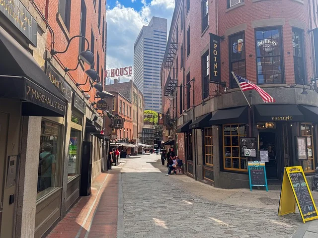
Boston is the biggest US chip design cluster outside Silicon Valley, and the center of gravity is analog. Analog Devices runs its headquarters in Wilmington, just north of the city, and its signal-processing and power-management IC teams are the reason a lot of analog engineers end up in Massachusetts in the first place.
ASIC work in the area is split across a few recognizable names. Marvell runs a networking ASIC design center in Andover. Raytheon, MITRE, and MIT Lincoln Laboratory do defense-grade ASICs, which means clearances, long programs, and parts that have to survive environments commercial silicon never sees. Draper Laboratory sits in the same world. Then there is the startup layer around MIT and Kendall Square: Lightmatter on photonic AI computing in Cambridge, plus a rotating set of CSAIL spin-outs building accelerators.
What the job looks like depends heavily on which of those you join. At ADI it is precision analog and mixed-signal: data converters, amplifiers, power management, the kind of design where a few microvolts of offset matters. At Marvell Andover it is high-speed digital and SerDes for networking and storage controllers. At the defense shops it is rad-hard and secure design under a very different schedule. The startups want people comfortable owning a block end to end without a large methodology team behind them.
The talent pipeline is unusually dense for a metro this size. MIT and Harvard feed it directly, and the local VC base (Spark Capital, General Catalyst, Pillar) keeps funding new hardware teams, so engineers move between ADI, the defense labs, and startups more than you would expect. If you want to stay in analog for a whole career, Boston and Dallas are the two US metros where you can do it without relocating every few years.
Compensation tracks the national ASIC market, with the usual Boston cost-of-living premium on top. For current figures by role and seniority, see our semiconductor salary guide.
For more local roles, check related listings in Boston semiconductor design and Analog Devices IC design. Set up a profile on semidesignjobs.com, turn on Boston ASIC alerts, and new openings land in your inbox as they post.
FAQ
Who are the top semiconductor employers in the Boston area?
Analog Devices, headquartered in Wilmington, MA, is the largest. Marvell runs a networking ASIC center in Andover. Draper Laboratory, MIT Lincoln Laboratory, and Raytheon handle defense ASICs, and there is a cluster of AI chip and quantum hardware startups spun out of MIT and Harvard.
Is Boston a good location for analog IC design engineers?
It is one of the two best US metros for analog IC design, along with Dallas. Analog Devices' headquarters is here, with deep teams in signal processing and power management, so analog engineers can build a long career without relocating. The MIT base also makes it easy to move into startup roles when you want a change.
What AI chip companies are growing in the Boston area?
Lightmatter, working on photonic AI computing in Cambridge, is the best known. Beyond it, the Kendall Square corridor has a rotating set of MIT CSAIL spin-outs building AI accelerator ASICs, usually backed by MIT researchers and local VCs. It is a smaller scene than the Bay Area, but it is active and tightly linked to the university labs.